Improve IC packaging quality with high‑resolution 2D inspection and deterministic image capture that fits your existing inspection cells
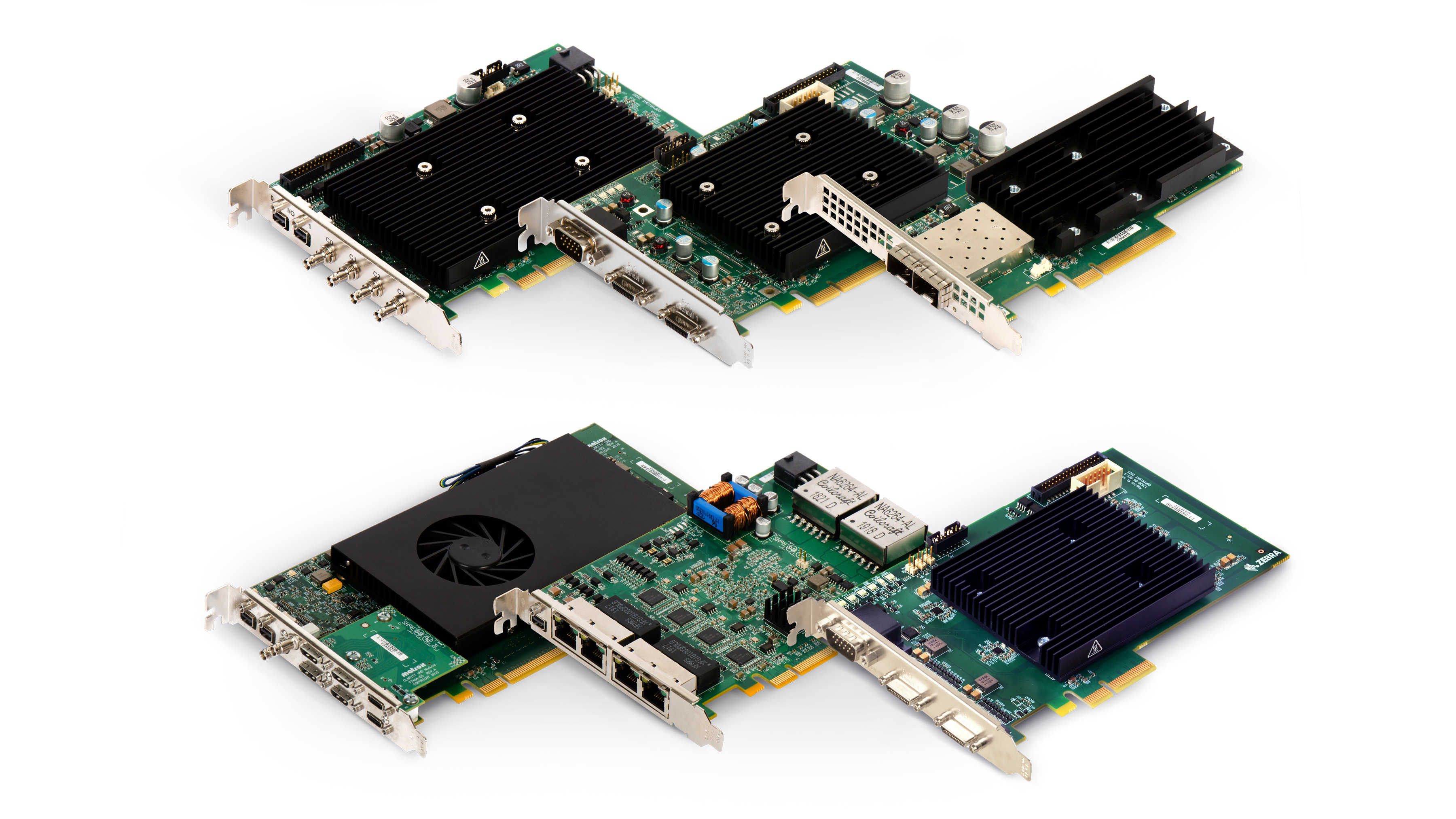
Capture ultra‑fine features at line speed
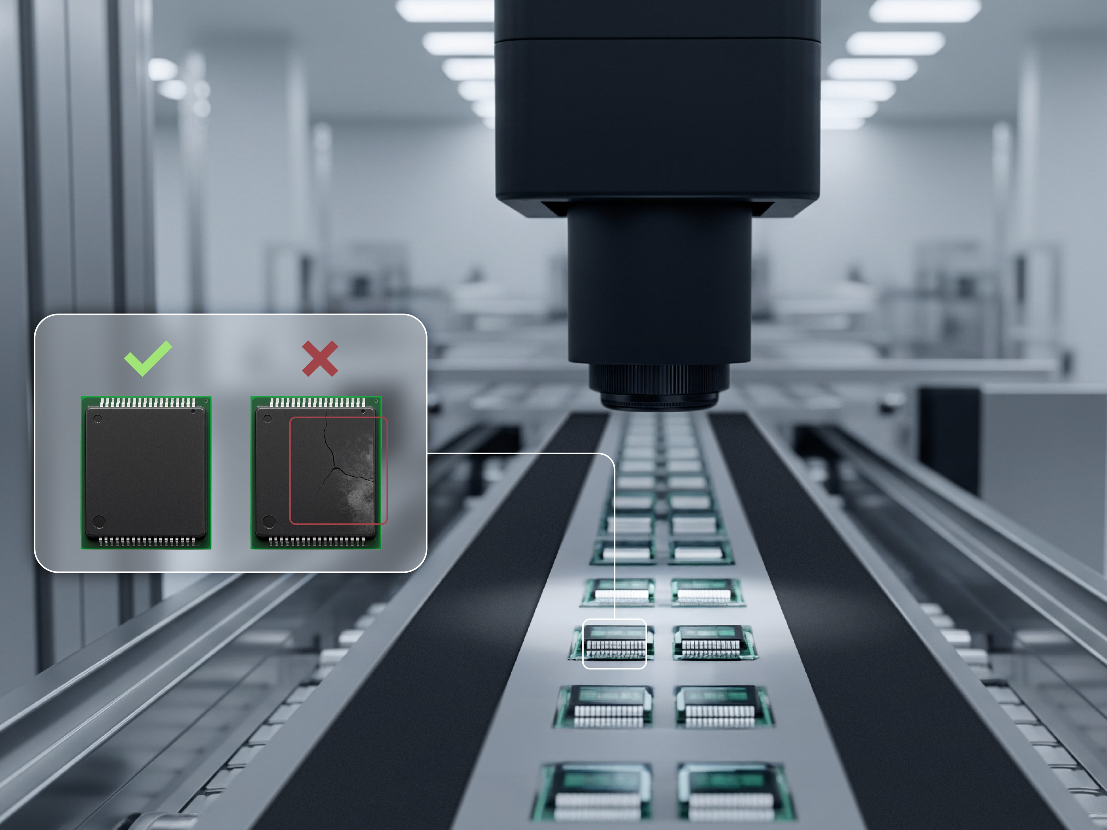
Zebra frame grabber cards pair with high‑resolution area‑scan or line‑scan cameras to capture crisp 2D images at full line speed, preserving fine print, edge contrast, and subtle surface texture on moulded packages. Rapixo CXP frame grabbers support CoaXPress up to CXP‑12 with PoCXP to power and acquire from one to four cameras, while Rapixo CL/CL Pro supports Camera Link 2.1, including Full/80‑bit modes, for deterministic acquisition with onboard FPGA offload and ample auxiliary I/Os for triggers and encoders. Deterministic triggering coordinates cameras and lighting, onboard buffering prevents drops, and multi‑camera sync covers top, side, and lead views under bright‑field, dark‑field, or coaxial illumination.
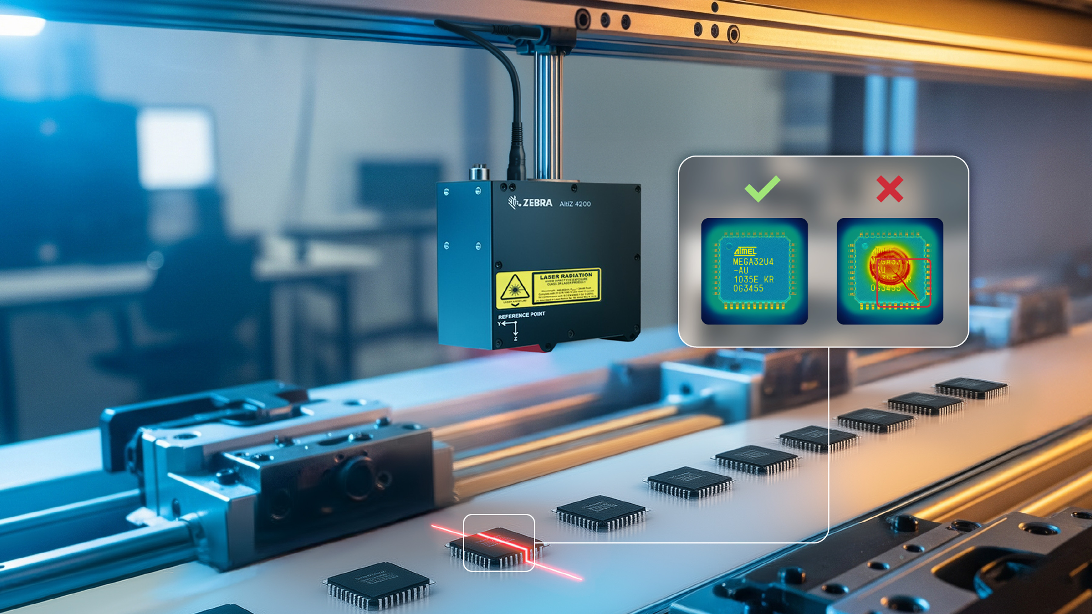
Add 3D profile inspection
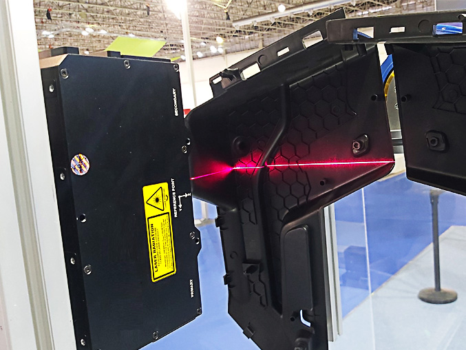
For coplanarity, standoff, warpage, and package topography that 2D can miss, integrate Zebra AltiZ 3D profile sensors. The AltiZ Series delivers ultra‑high resolution with more than 4,200 points per profile and capture rates up to 14,000 profiles per second, producing reliable depth maps and point clouds for precise lead‑tip height, package bow, and mark relief checks at semiconductor line speeds. Its dual‑camera, single‑laser design reduces occlusions at critical surface junctures, while an IP67 housing, GigE Vision with PoE, encoder inputs, and M12 I/O simplify deployment in harsh, space‑constrained cells and enable multi‑sensor synchronisation for full top/side coverage.
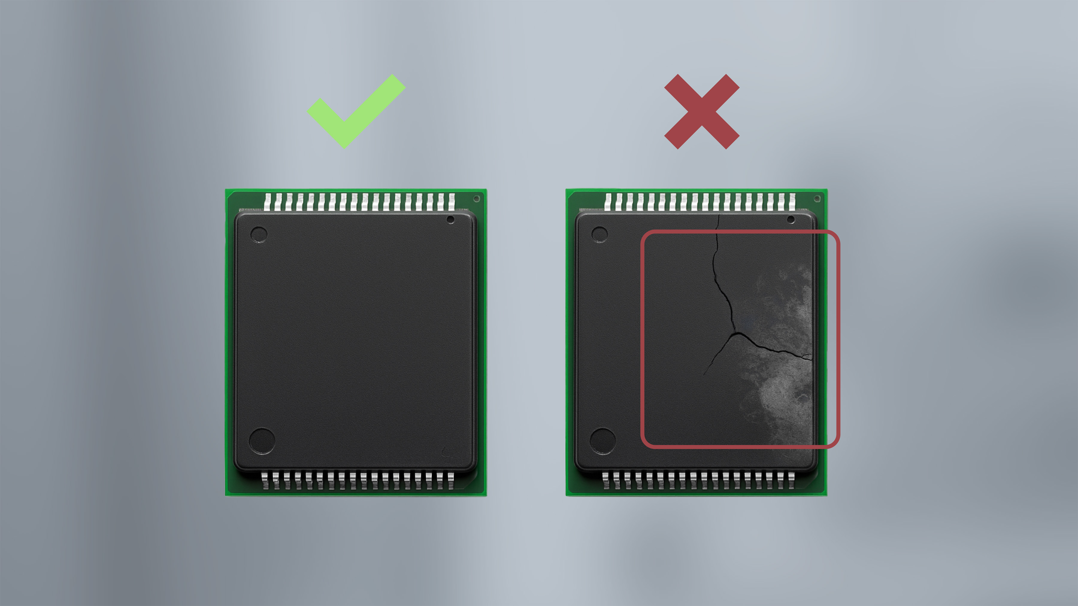
Automating chip packaging quality checks
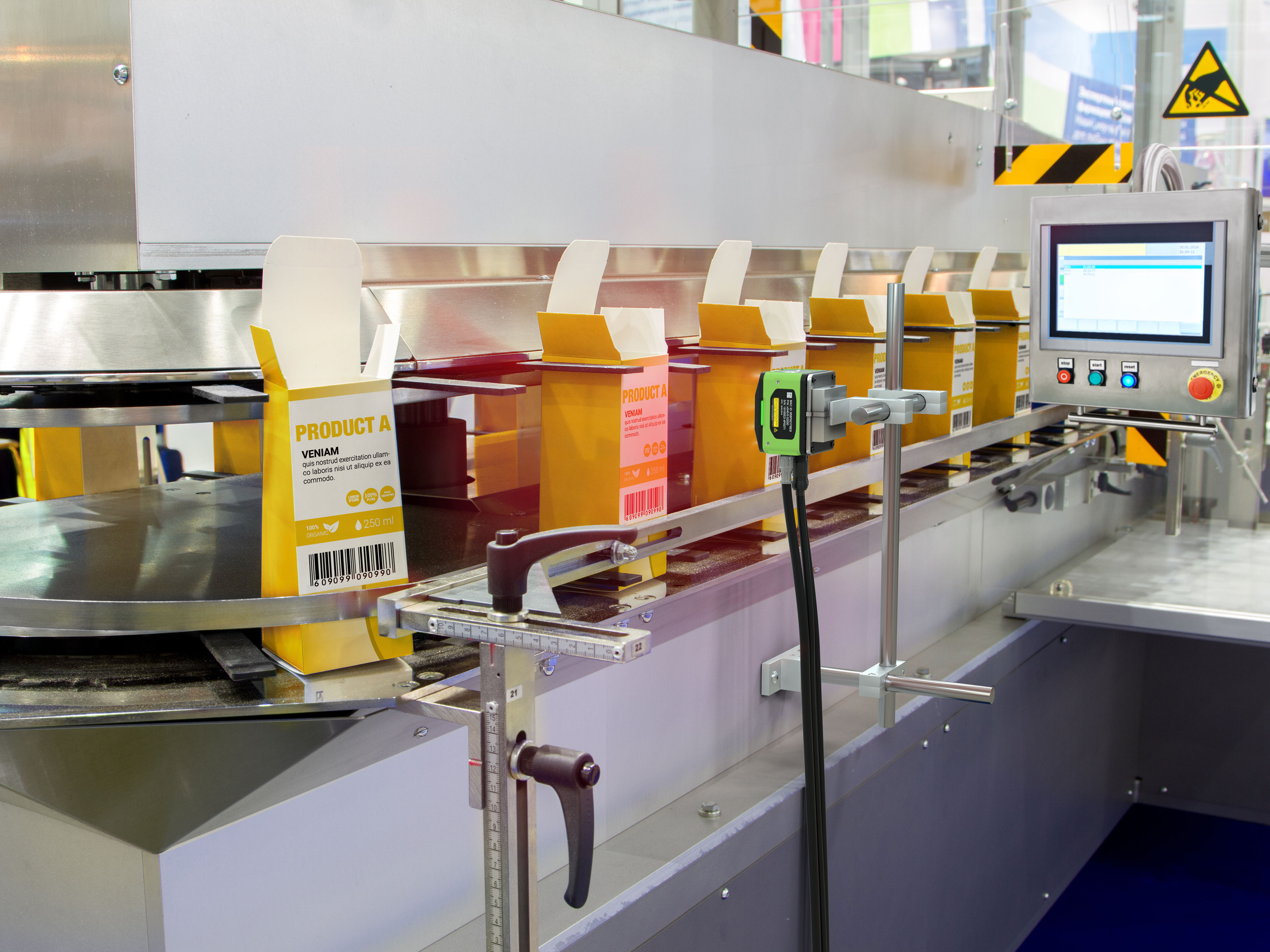
Zebra Aurora Design Assistant streamlines application development and changeover with a flowchart‑based IDE that builds inspection logic without traditional coding, designs a web‑based HMI for operators, and runs multi‑camera projects on PCs and controllers using CoaXPress, GigE Vision, or USB3 Vision. It integrates communications for PLCs and MES via discrete I/O and industrial protocols such as EtherNet/IP, PROFINET, Modbus, OPC UA, and TCP/IP, so pass/fail, defect types, and measurements drive reject gates, part marking, and traceability. Deep learning-based OCR and object detection, combined with classical metrology, pattern matching, and OCR/OCV, enable robust mark verification and dimensional checks. Recipe/version control, runtime monitoring, and profiling utilities also support auditability and continuous improvement.
