Transform retail operations with Zebra’s retail technology solutions, featuring hardware and software for improving inventory management and empowering teams.
Streamline operations with Zebra’s healthcare technology solutions, featuring hardware and software to improve staff collaboration and optimise workflows.
Enhance processes with Zebra’s manufacturing technology solutions, featuring hardware and software for automation, data analysis, and factory connectivity.
Zebra’s transportation and logistics technology solutions feature hardware and software for enhancing route planning, visibility, and automating processes.
Zebra's hospitality technology solutions equip your hotel and restaurant staff to deliver superior customer and guest service through inventory tracking and more.
Zebra's market-leading solutions and products improve customer satisfaction with a lower cost per interaction by keeping service representatives connected with colleagues, customers, management and the tools they use to satisfy customers across the supply chain.
Empower your field workers with purpose-driven mobile technology solutions to help them capture and share critical data in any environment.
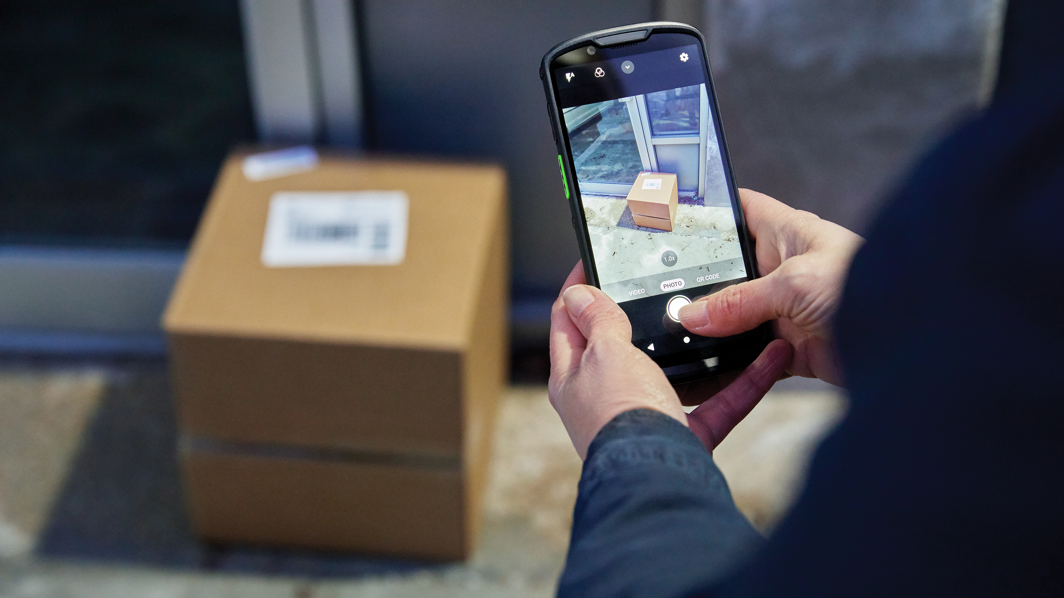
Zebra's range of mobile computers equip your workforce with the devices they need from handhelds and tablets to wearables and vehicle-mounted computers.
Zebra's desktop, mobile, industrial, and portable printers for barcode labels, receipts, RFID tags and cards give you smarter ways to track and manage assets.
Zebra's 1D and 2D corded and cordless barcode scanners anticipate any scanning challenge in a variety of environments, whether retail, healthcare, T&L or manufacturing.
Zebra's extensive range of RAIN RFID readers, antennas, and printers give you consistent and accurate tracking.
Choose Zebra's reliable barcode, RFID and card supplies carefully selected to ensure high performance, print quality, durability and readability.
Zebra's rugged tablets and 2-in-1 laptops are thin and lightweight, yet rugged to work wherever you do on familiar and easy-to-use Windows or Android OS.
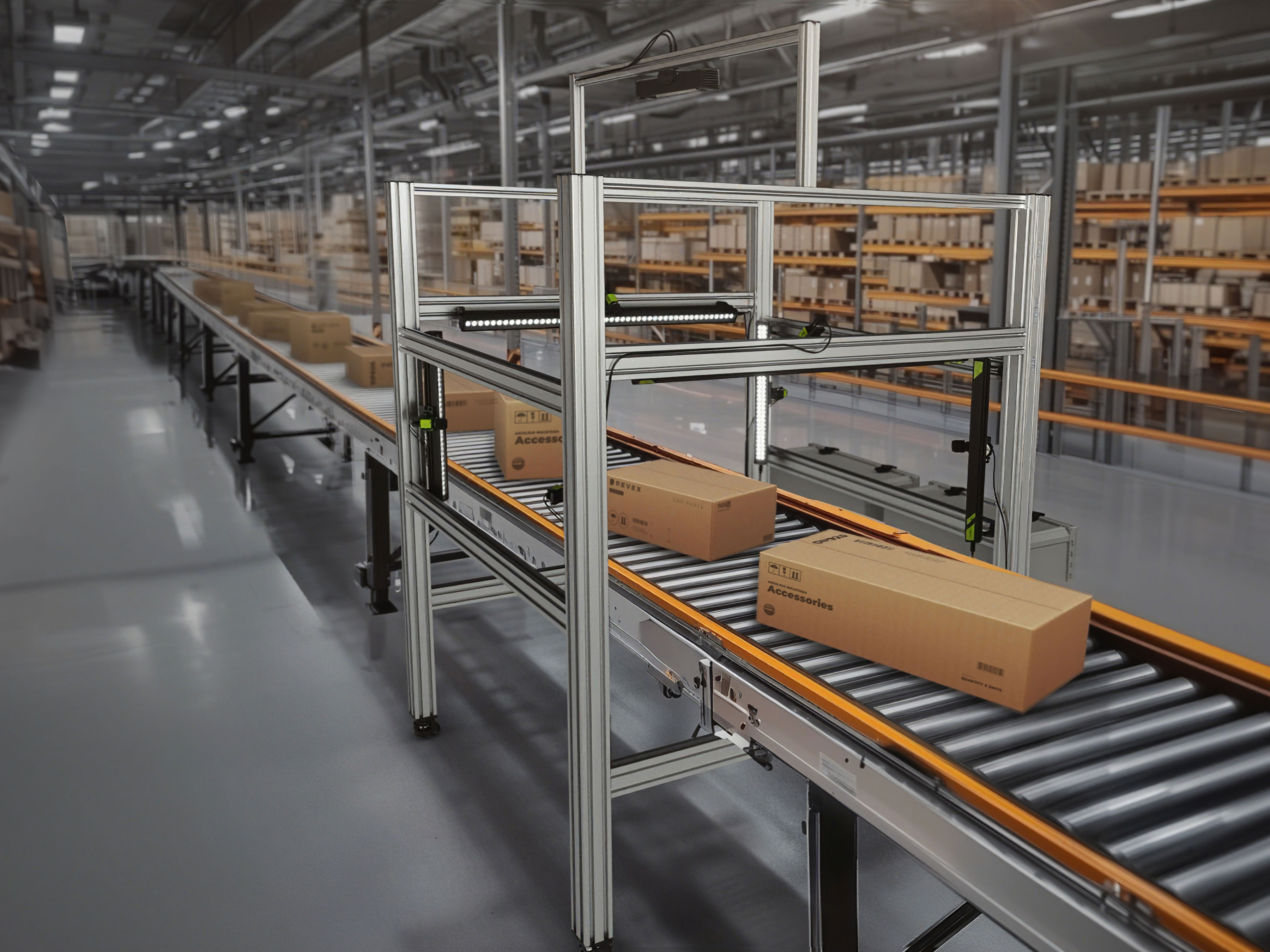
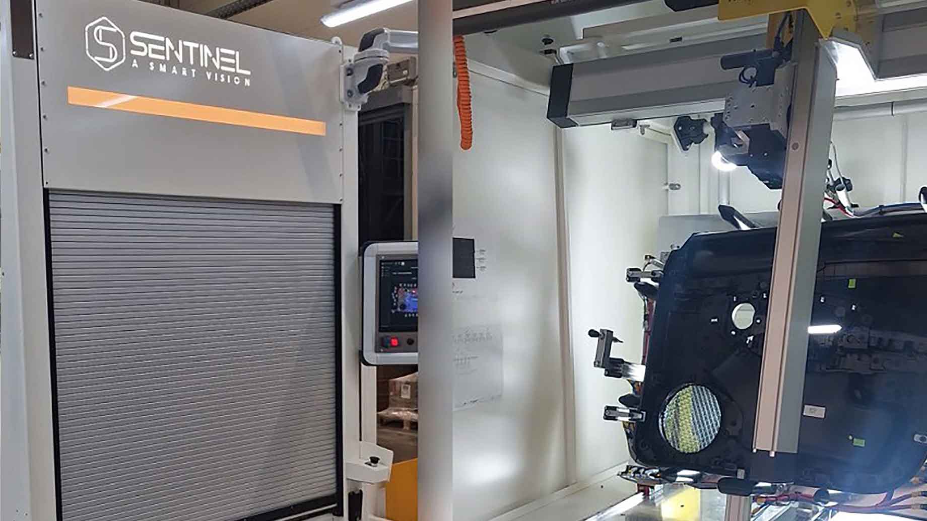
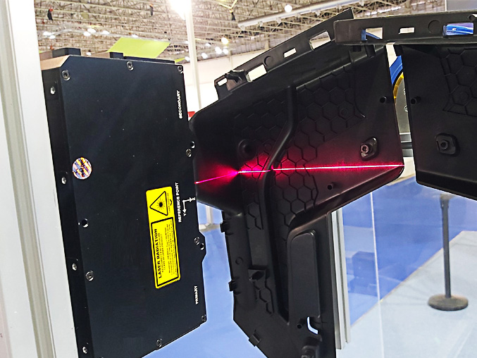
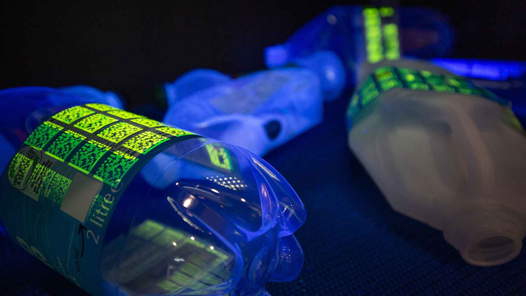
With Zebra's family of fixed industrial scanners and machine vision technologies, you can tailor your solutions to your environment and applications.
Zebra’s line of kiosks can meet any self-service or digital signage need, from checking prices and stock on an in-aisle store kiosk to fully-featured kiosks that can be deployed on the wall, counter, desktop or floor in a retail store, hotel, airport check-in gate, physician’s office, local government office and more.
Discover Zebra’s range of accessories from chargers, communication cables to cases to help you customise your mobile device for optimal efficiency.
Zebra's environmental sensors monitor temperature-sensitive products, offering data insights on environmental conditions across industry applications.
Zebra's location technologies provide real-time tracking for your organisation to better manage and optimise your critical assets and create more efficient workflows.
Enhance frontline operations with Zebra’s AI software solutions, which optimize workflows, streamline processes, and simplify tasks for improved business outcomes.
Empower your frontline with Zebra Companion AI, offering instant, tailored insights and support to streamline operations and enhance productivity.
Boost productivity with Zebra Frontline AI Enablers: AI vision models, sample apps, and APIs streamline workflows for efficient business processes.
Zebra Frontline AI Blueprints deliver adaptable, real-world AI frameworks that automate manual tasks and drive efficiency in high-pressure frontline operations.
Zebra Workcloud, enterprise software solutions boost efficiency, cut costs, improve inventory management, simplify communication and optimize resources.
Keep labour costs low, your talent happy and your organisation compliant. Create an agile operation that can navigate unexpected schedule changes and customer demand to drive sales, satisfy customers and improve your bottom line.
Drive successful enterprise collaboration with prioritized task notifications and improved communication capabilities for easier team collaboration.
Get full visibility of your inventory and automatically pinpoint leaks across all channels.
Reduce uncertainty when you anticipate market volatility. Predict, plan and stay agile to align inventory with shifting demand.
Drive down costs while driving up employee, security, and network performance with software designed to enhance Zebra's wireless infrastructure and mobile solutions.
Explore Zebra’s printer software to integrate, manage and monitor printers easily, maximising IT resources and minimising down time.
Make the most of every stage of your scanning journey from deployment to optimisation. Zebra's barcode scanner software lets you keep devices current and adapt them to your business needs for a stronger ROI across the full lifecycle.
RFID development, demonstration and production software and utilities help you build and manage your RFID deployments more efficiently.
RFID development, demonstration and production software and utilities help you build and manage your RFID deployments more efficiently.
Zebra DNA is the industry’s broadest suite of enterprise software that delivers an ideal experience for all during the entire lifetime of every Zebra device.
Advance your digital transformation and execute your strategic plans with the help of the right location and tracking technology.
The Zebra Aurora suite of machine vision software enables users to solve their track-and-trace, vision inspection and industrial automation needs.
Zebra Aurora Focus brings a new level of simplicity to controlling enterprise-wide manufacturing and logistics automation solutions. With this powerful interface, it’s easy to set up, deploy and run Zebra’s Fixed Industrial Scanners and Machine Vision Smart Cameras, eliminating the need for different tools and reducing training and deployment time.
Aurora Imaging Library™, formerly Matrox Imaging Library, machine-vision software development kit (SDK) has a deep collection of tools for image capture, processing, analysis, annotation, display, and archiving. Code-level customisation starts here.
Aurora Design Assistant™, formerly Matrox Design Assistant, integrated development environment (IDE) is a flowchart-based platform for building machine vision applications, with templates to speed up development and bring solutions online quicker.
Designed for experienced programmers proficient in vision applications, Aurora Vision Library provides the same sophisticated functionality as our Aurora Vision Studio software but presented in programming language.
Aurora Vision Studio, an image processing software for machine & computer vision engineers, allows quick creation, integration & monitoring of powerful OEM vision applications.
Adding innovative tech is critical to your success, but it can be complex and disruptive. Professional Services help you accelerate adoption, and maximise productivity without affecting your workflows, business processes and finances.
Zebra's Managed Service delivers worry-free device management to ensure ultimate uptime for your Zebra Mobile Computers and Printers via dedicated experts.
Find ways you can contact Zebra Technologies’ Support, including Email and Chat, ask a technical question or initiate a Repair Request.
Zebra's Circular Economy Program helps you manage today’s challenges and plan for tomorrow with smart solutions that are good for your budget and the environment.
Measuring Wafer Position
Handling wafers is a precise task where even the slightest misalignment can cause issues during the lithography process, leading to longer changeovers and lower yields. Vision-guided inspections offer high-resolution imaging and precise measurements. Adding 3D sensing verifies the position, tilt, and orientation of wafers while in motion, helping robots avoid touching fragile surfaces. Automated, in-line controls enhance quality, speed up cycles, and improve yields.
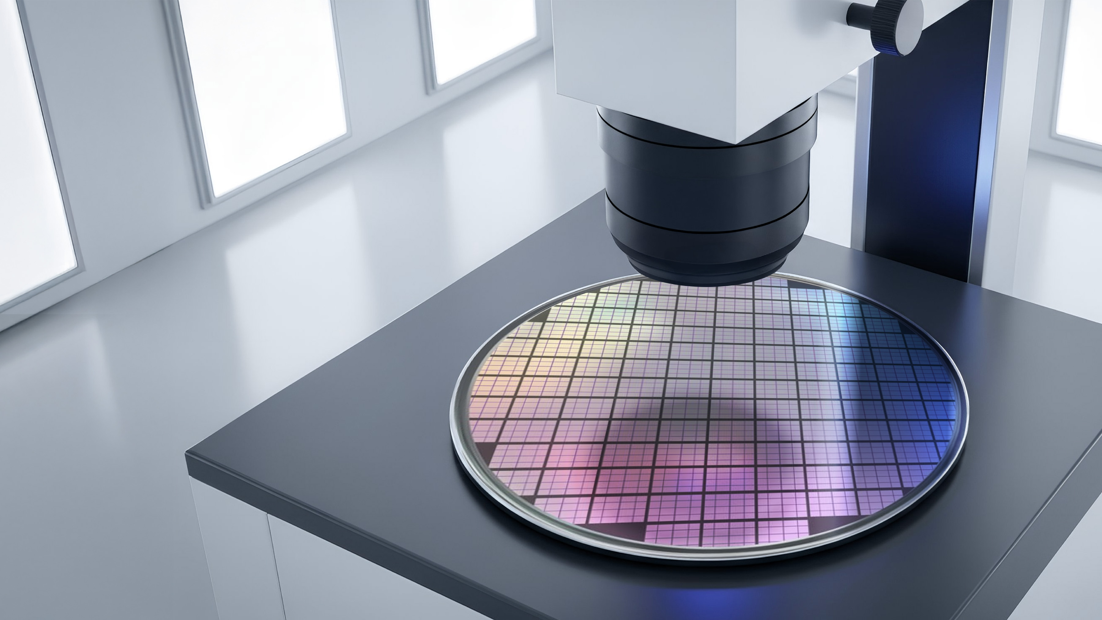
Confidently measure wafer notch position using 2D imaging and 3D validation for faster lines and improved yield
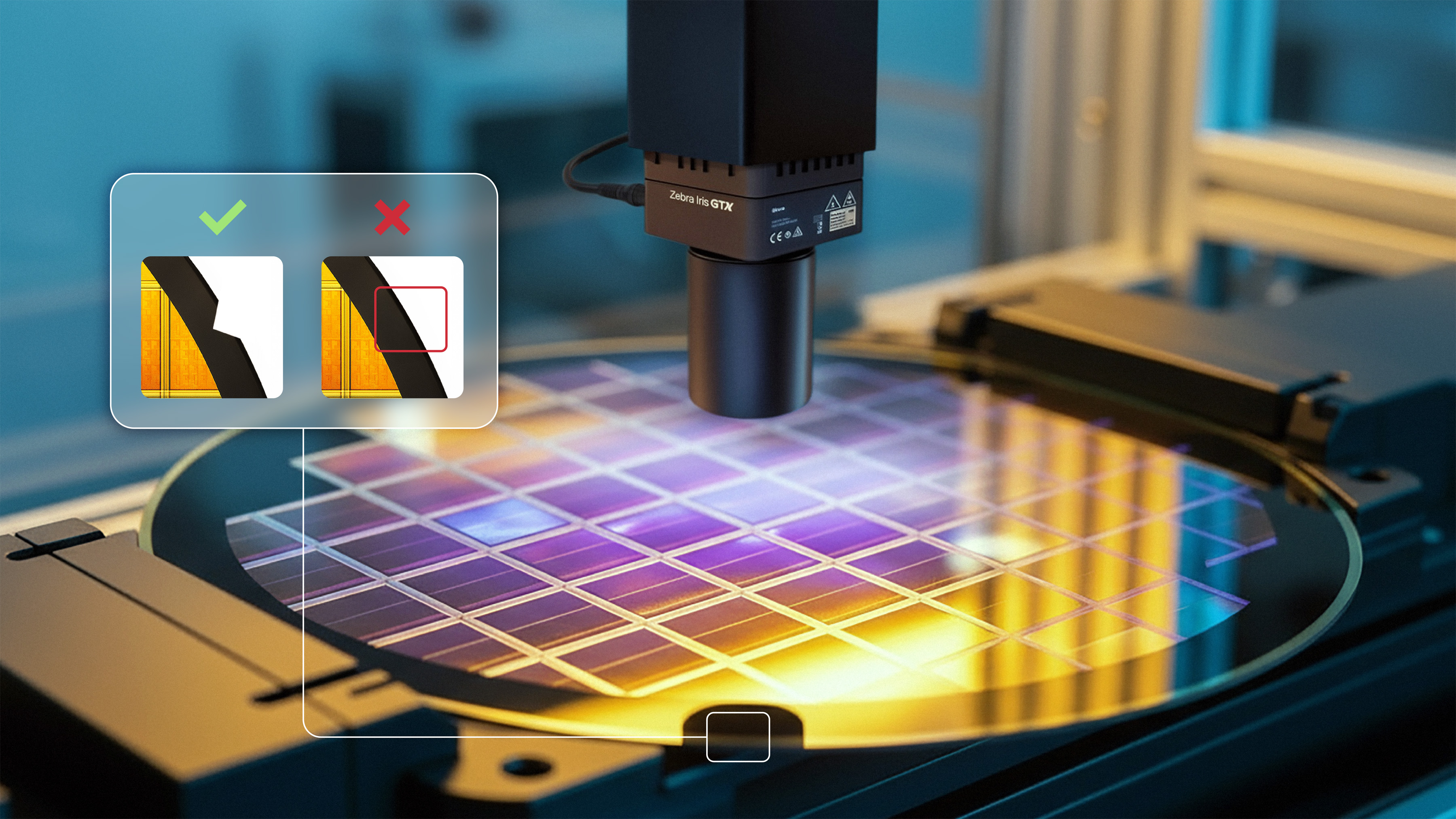
Measure wafer notch position with precision
Zebra smart cameras capture high-resolution images of the wafer’s edges and notches. These images are analysed using Aurora machine vision software. After calibrating the optics once, the software converts the pixel distances into micrometers. It then matches arcs, lines, and circle centres to the wafer’s edge to determine the notch’s angle and offset, checking these against user-defined tolerances. If there’s any misalignment, a correction to adjust the wafer can be made before the next step, ensuring it stays precisely aligned.
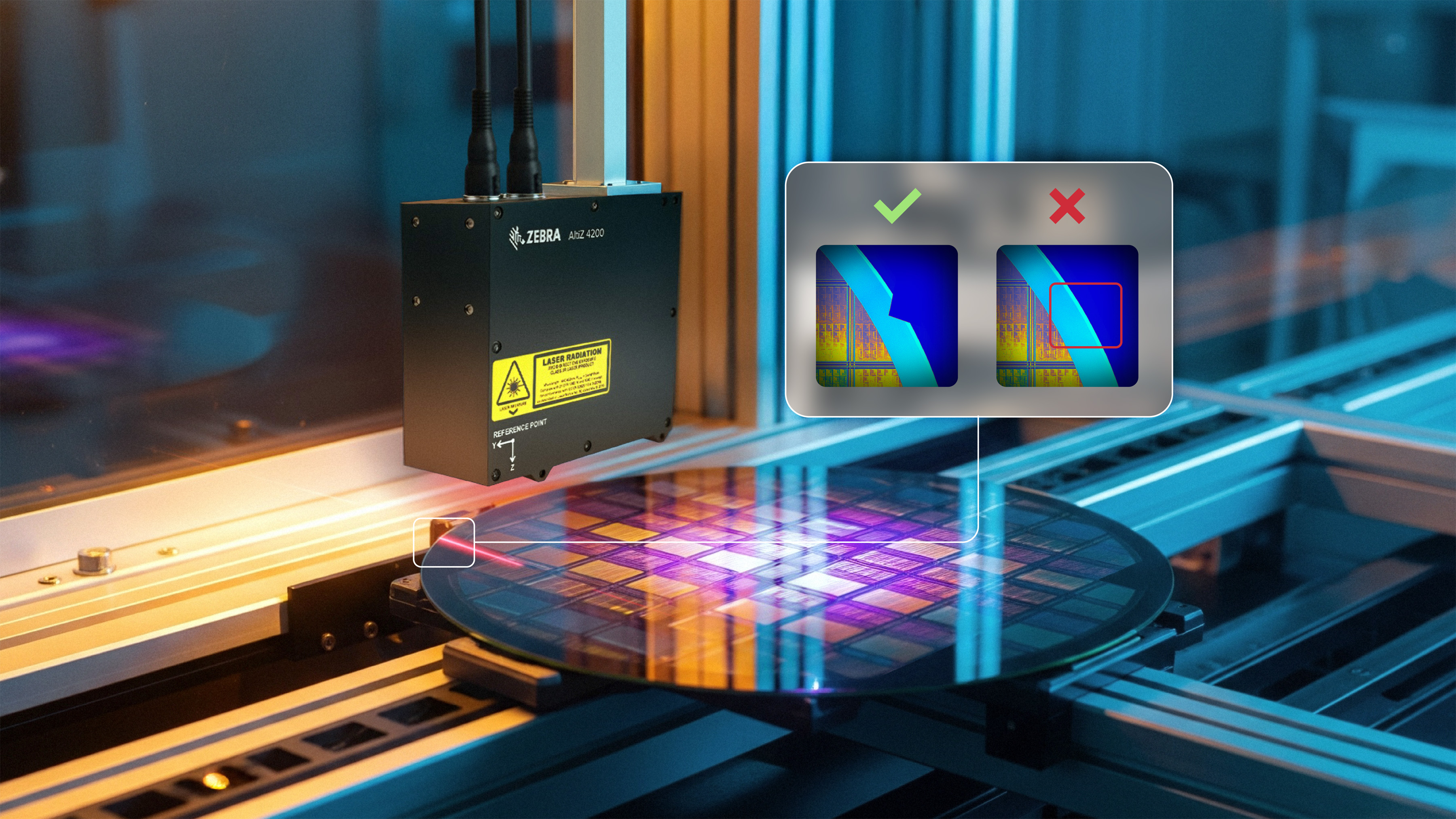
Add 3D validation for in‑motion accuracy
AltiZ 3D profile sensors capture three‑dimensional (3D) point clouds of the wafer edge and notch while conveyors move, verifying the wafer’s position, tilt, and bow without stopping the line. The system cross-checks 2D measurements with 3D geometry to prevent errors from glare, automatically adjusting robot handling or raising alarms as needed. It effectively manages glossy surfaces and maintains alignment at typical production speeds.
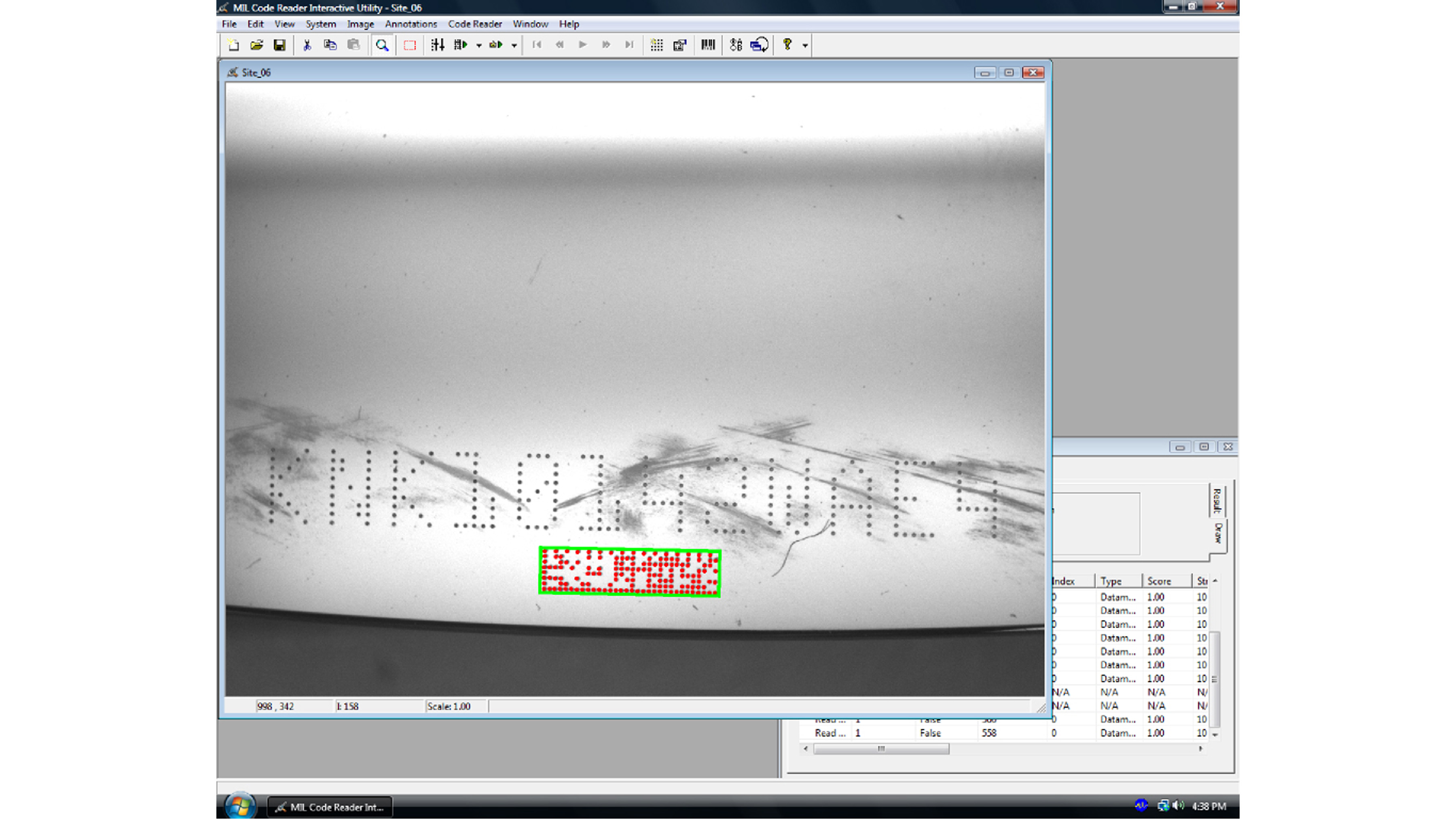
Turn Inspection Data into Process Control and Traceability
The Zebra Aurora software platform makes it easy to share alignment results directly with a Manufacturing Execution System (MES) and statistical process control (SPC) dashboards. Aurora Imaging Library software captures precise measurements of wafer positions. Each measurement is carefully tagged with information like lot, tool, and recipe IDs, making audits traceable and allowing for strong trend analysis. This all-in-one solution ensures that wafers meet strict quality standards, automatically flags out-of-spec positions, and keeps a detailed record of any adjustments made.
Related Use Cases
Fixed Industrial Scanning and Machine Vision Success Stories
Legal Terms of Use Privacy Policy Supply Chain Transparency
ZEBRA and the stylized Zebra head are trademarks of Zebra Technologies Corp., registered in many jurisdictions worldwide. All other trademarks are the property of their respective owners. Note: Some content or images on zebra.com may have been generated in whole or in part by AI. ©2026 Zebra Technologies Corp. and/or its affiliates.
